
How are SWIR imagers used in the semiconductor & solar cell industry?
SWIR imagers were initially used in the telecommunications industry as they are sensitive to the 1550 nm light typically used in optical fibres. Nowadays, SWIR imaging is used in a wide variety of applications in semiconductor and solar cell industry:
Emission microscopy: Photon emission microscopy, or electroluminescence imaging, is a relatively new failure analysis technique for detecting photonic radiation from a defect site, primarily due to carrier recombination mechanisms.
Failure analysis: Targeted failure analysis as applied in microelectronics is usually carried out in a five-step sequence: First is fault validation, followed by localizing the defect. Then the defect location is prepared and traced for analysis; the nature of the defect is determined and, finally, an investigation of its root causes is initiated.
Solar cell inspection: SWIR imaging enables you to look “through” the silicon wafer and therefore allows inspection of defects and failures of solar cells, which cannot be detected and visualized by other methods.
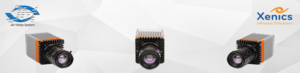
What do we offer?
We offer the Bobcat-series for these applications.
Our Bobcat-320, Bobcat-640-CL & Bobcat-640-GigE are very small and lightweight SWIR InGaAs cameras. They consume very little power and are cheaper than other cooled SWIR cameras. Therefore, customers continuously find new applications for system integration where cost, size and power are critical. The Bobcat answer to the need of flexibility in terms of data and control interfaces with its GigE or CameraLink interface.